X-ES Introduces the XCalibur5090 6U Digital Signal Processing Module with Dual Xilinx Virtex-7 FPGAs
Middleton, WI—Mon, Oct 12th, 2015
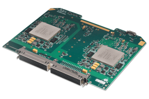
Extreme Engineering Solutions, Inc. (X-ES) announces the XCalibur5090, a dual Xilinx Virtex-7 based Digital Signal Processing (DSP) 6U LRM FPGA module featuring high-speed serial interfaces, DAC and ADC channels, external memory, and flexible, high-density I/O for customizable, high-bandwidth, signal-processing applications.
Rapid Signal Processing from a Rugged 6U FPGA Module
Available in a rugged, conduction-cooled 6U LRM form factor, XCalibur5090 is fully-capable of signal processing in the most harsh environments and extreme applications. Each user-programmable Xilinx Virtex-7 XC7VX690T FPGA is coupled with a single 12-bit ADC chip, configured as a single 3.2 GSPS input or dual 1.6 GSPS inputs, and two 14-bit DAC output chips, configured as 2.5 GSPS outputs.
These closely coupled ADC and DAC chips result in very low latency between inputs and outputs, making it ideal for applications like electronic warfare (EW) and SDR (Software Defined Radio), where a signal will need to be received and then rapidly transmitted. Channels can be synchronized to form an array of synchronized analog inputs, serving a critical need for applications like SIGINT that require beamforming.
Each FPGA supports two banks of 32-bit, 1 GB DDR3-1600 SDRAM connected directly to the FPGA. This provides significant flexibility for applications using memory and read or write bandwidths >5 GB/s for each bank. With support for commercial and industrial temperature, as well as -1, -2, and -3 speed grades, the XCalibur5090 is a versatile, reconfigurable FPGA module well-suited to a diverse array of signal-processing and logic demands.
Firmware Development Kit (FDK) Available
An X-ES Firmware Development Kit (FDK) is available with the XCalibur5090, which provides an example design and IP blocks for each interface including the ADC and DAC, all using the AXI interface. Consisting of a proven example design, HDL, and software functions, the FDK accelerates developing FPGA algorithms and logic for X-ES customer-programmable FPGA products. Designed to be easily extended, the FDK allows the developer to concentrate on their application development and not the integration of the hardware interface. In addition, the FDK facilitates simulation and verification of the hardware using the provided example design and test benches.
MCOTS Solutions from X-ES
X-ES excels at offering MCOTS (Modified COTS) versions of our standard, Commercial-Off-The-Shelf products. When engineering boards such as the XCalibur5090, we go to great lengths to determine how its design and layout will translate to a variety of other form factors. When laying out the PCB, each section is treated in a modular fashion to achieve design efficiencies later on in MCOTS designs – this allows for design segments to easily be adapted to additional form factors with minimal modification. X-ES’ focus on design efficiency in the standard product core design stage for critical sections such as memory and I/O routing allows us to then be highly-versatile and provide shorter lead times on getting an MCOTS product from conception to the field.

Contact X-ES today for more information on the XCalibur5090, or on our MCOTS solutions for your next project.