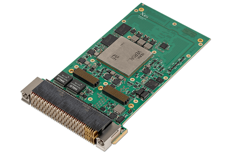
The XPedite2870 is a high-performance, reconfigurable, conduction-cooled 3U VPX processing module based on the AMD Versal® Gen 2 adaptive system-on-chip (ASoC). With multiple high-speed fabric interfaces and 32 GB of four-channel LPDDR5x SDRAM with in-band ECC, the XPedite2870 is well suited for customizable, high-bandwidth signal-processing applications. It combines X-ES SecureCOTS™ technology with either a Versal Gen 2 AI Edge 2VE3858 or Prime 2VM3858 ASoC, enabling custom functions that help protect data from unauthorized modification or observation. This makes the XPedite2870 an ideal platform for applications with stringent security requirements.
The module provides a pinout compatible with the Sensor Open Systems Architecture (SOSA) I/O Intensive profile SLT3-PAY-1F1F2U1TU1T1U1T-14.2.16) and is also designed to support SOSA-aligned AMPS profile MODA3-16.2.15-1-F2C-(P4F)(P4F)(2E7-E3)(N-D1-U1-N-M3/M4/M5-N).
As a heterogeneous compute platform, the XPedite2870 combines eight Arm Cortex®-A78AE application processor cores, 10 Arm Cortex-R52 real-time processor cores, a quad-core Arm Mali™-G78AE GPU, a high-bandwidth Network-on-Chip (NoC) interconnect, and a large programmable-logic fabric. When configured with the Versal Gen 2 AI Edge device, the platform also incorporates AI Engines that provide additional acceleration for machine-learning inference, signal processing, and other highly parallel compute workloads. These specialized processing resources support demanding applications including packet processing, signal processing, sensor I/O, DSP-intensive workloads, next-generation 5G wireless infrastructure, image classification, real-time situational awareness, and aerospace and defense systems.
For high-speed connectivity, the XPedite2870 provides two x4 and two x1 High-Speed Serial (HSS) interfaces capable of operating at up to 25 Gbps, along with two 10/100/1000BASE-T Ethernet ports. The module supports up to 256 GB of onboard NAND flash and provides a broad range of additional backplane I/O, including LVDS, single-ended GPIO, and RS-232/422/485 serial interfaces.
An integrated XMC site provides additional expansion capability. The XMC interface includes one x4 PCI Express Gen5-capable connection, capable of operating at up to 32 Gbps to the Versal Gen 2 ASoC, as well as X12d I/O routed directly to the VPX backplane connectors. Optional configurations can also route x16s and x8d interfaces from the XMC site to the VPX backplane.
The XPedite2870 delivers a feature-rich, high-performance platform for interfacing with and processing streaming data from a wide variety of sensors. The X-ES FPGA Development Kit (FDK) provides a pre-validated environment for rapid application development, including an optimized IP library, design resources, software components, and complete example designs for the XPedite2870. The development environment also includes the Arm Trusted Firmware (ATF) and the U-Boot bootloader. Linux Yocto support is available separately.